
SEMICONDUCTORS Lesson Note
LEARNING OBJECTIVES:
This SS3 Physics lesson note covers SEMICONDUCTORS for First Term, Week 3.
Lesson Note
LEARNING OBJECTIVES:
By end of lesson, students should be able to:
1. Define semiconductor
2. Distinguish conductors, semiconductors and insulators by energy band
3. Explain intrinsic and extrinsic semiconductors
4. Explain doping, p-type and n-type semiconductors
5. Explain p-n junction and its uses
A. DEFINITION OF SEMICONDUCTOR
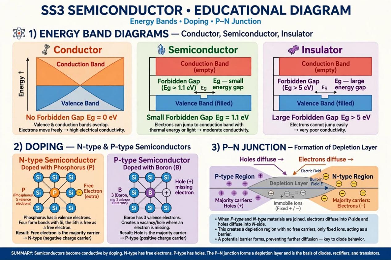
A semiconductor is a material whose conductivity is between that of a good conductor (e.g copper, aluminum) and a good insulator (e.g glass, rubber). They are widely used in the electronic industry. Semi-conductor materials possess crystalline structure i.e the atom are arranged in an orderly manner.
Its conductivity increases with temperature, unlike metals.
Examples: Silicon (Si) and Germanium (Ge) are the most common. Others are Gallium Arsenide (GaAs), Silicon Carbide.
ENERGY BAND THEORY:
Why some metals conduct and some don't
Every solid has two bands:
i) Valence band: Band filled with valence electrons. Electrons here are bound.
ii) Conduction band: Empty band where electrons are free to conduct.
iii) Forbidden gap / Energy gap ( Eg): Gap between valence and conduction band.
Conductors: Valence and conduction bands overlap, Eg = 0. Electrons move freely. e.g Cu, Al
Semiconductors: Small forbidden gap
Eg 1eV. For Si Eg = 1.1eV, Ge Eg = 0.7eV. At 0K it behaves as insulator, at room temp some electrons jump to conduction band and conduct.
- Insulators: Large forbidden gap e.g. 5-10eV. e.g. glass, rubber. Electrons cannot jump.
3. TYPES OF SEMICONDUCTORS
A. INTRINSIC SEMICONDUCTOR (Pure)
This is a pure semiconductor with no impurity added. e.g Pure Silicon, Pure Germanium.
At 0K, no conduction. As temperature rises, covalent bonds break and create:
- Electron in conduction band (negative charge)
- Hole in valence band (positive charge, absence of electron)
Number of electrons = Number of holes.
ne = nh
Conductivity is low.
B. EXTRINSIC SEMICONDUCTOR (Impure/Doped)
This is a semiconductor whose conductivity has been improved by adding small impurity. The process of adding impurity is called DOPING.
Doping is done with elements from Group 3 or Group 5 of periodic table.
There are two type
i) N-TYPE SEMICONDUCTOR (Negative Type)
- Formed by doping intrinsic semiconductor (Si) with pentavalent impurity (5 valence electrons) e.g Phosphorus (P), Arsenic (As), Antimony (Sb).
- 4 electrons form covalent bond with Si, 1 electron is free to move.
- Majority carriers = Electrons (negative)
- Minority carriers = Holes
ii) P-TYPE SEMICONDUCTOR (Positive Type)
- Formed by doping with trivalent impurity (3 valence electrons) e.g Boron (B), Aluminium (Al), Gallium (Ga), Indium (In).
- 3 electrons bond with Si, creating one vacancy called hole.
- Majority carriers = Holes (positive)
- Minority carriers = Electrons
NB.: P for Positive - doped with 3, N for Negative - doped with 5.
P-N JUNCTION
A p- type an n-type semi-conductor crystal joined together to act as a single semi-conductor called is P-n junction. They can function like thermonic diode.
At the junction:
- Electrons from n side diffuse to p side
- Holes from p side diffuse to n side
- This creates a region with no free carriers called Depletion layer / Depletion region
- The depletion layer creates a barrier potential: 0.7V for Si, 0.3V for Ge. This opposes further diffusion.
P-N Junction as Diode:
It allows current to flow only in one direction.
ADVANTAGES OF SEMICONDUCTORS OVER VACUUM TUBES
1. Small size and light weight
2. Low power consumption
3. No heating required
4. Long life and rugged
5. Instant operation
6. Cheap
APPLICATIONS / USES OF SEMICONDUCTORS
1. Diodes: Rectification (changing AC to DC)
2. Transistors: Amplification, switching, in computers, phones, radios
3. Integrated Circuits (ICs): Thousands of components in one chip
4. Solar cells / Photodiodes: Convert light to electricity
5. Light Emitting Diodes (LEDs): Torch, screens, indicator lights
6. Thermistors: Temperature sensors
Evaluation
OBJECTIVE QUESTIONS
1. A material whose conductivity lies between conductor and insulator is called:
A) Superconductor
B) Semiconductor
C) Insulator
D) Electrolyte
2. The most commonly used semiconductors are:
A) Copper and Aluminum
B) Silicon and Germanium
C) Glass and Rubber
D) Iron and Zinc
3. The energy gap of a semiconductor is approximately:
A) 0 eV
B) ∼1 eV
C) ∼5-10 eV
D) 100 eV
4. At absolute zero (0K), an intrinsic semiconductor behaves as:
A) Conductor
B) Insulator
C) Superconductor
D) n-type
5. The process of adding impurity to a pure semiconductor to increase its conductivity is called:
A) Etching
B) Doping
C) Biasing
D) Rectification
6. An n-type semiconductor is formed by doping pure Silicon with:
A) Trivalent impurity like Boron
B) Pentavalent impurity like Phosphorus
C) Tetravalent impurity
D) No impurity
7. In p-type semiconductor, the majority charge carriers are:
A) Electrons
B) Holes
C) Protons
D) Neutrons
8. The region at p-n junction that has no free charge carriers is called:
A) Conduction band
B) Depletion layer
C) Valence band
D) Saturation region
9. The barrier potential for Silicon p-n junction is approximately:
A) 0.3 V
B) 0.7 V
C) 1.5 V
D) 5 V
10. Which of these is NOT an application of semiconductors?
A) Transistor
B) Diode
C) Integrated Circuit
D) Bicycle chain
Theory Questions
1a) Define semiconductor and differentiate between conductor, semiconductor and insulator using energy band theory.
b) Explain intrinsic and extrinsic semiconductors.
c) With examples of dopants, differentiate between n-type and p-type semiconductors stating their majority carriers.
2a) What is p-n junction? Explain formation of depletion layer and barrier potential.
b) State 3 advantages of semiconductors over vacuum tubes and 3 uses of semiconductors in everyday life.